

Artix7 Xilinx FPGA Development Board XC7A35T XC7A200T Core Board PCIe GTP
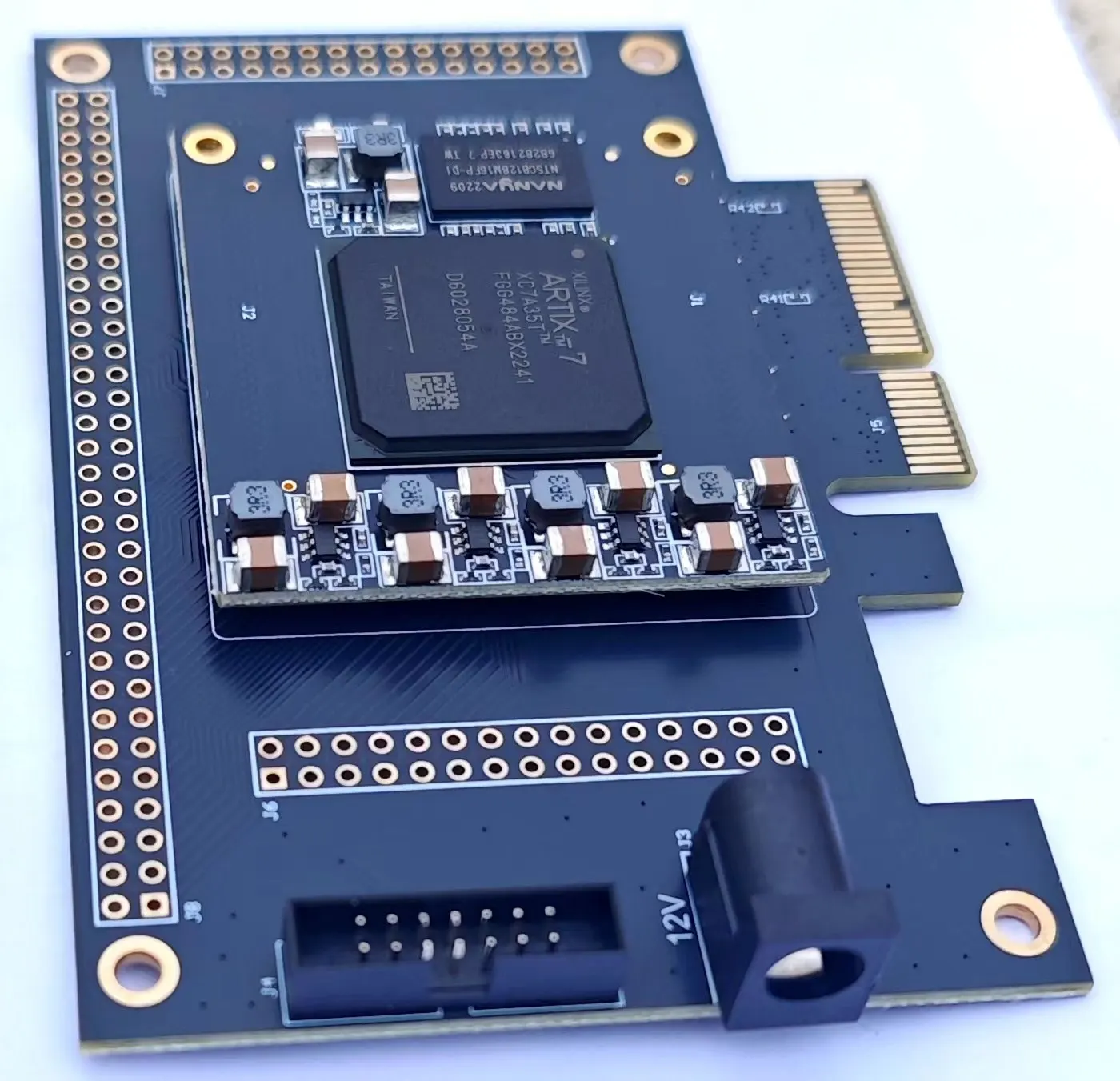
Test baseplate / XC7A200T Core Board
$891.90
Sale price
$891.90
Regular price
$0.00
Skip to product information


Artix7 Xilinx FPGA Development Board XC7A35T XC7A200T Core Board PCIe GTP
$891.90
Sale price
$891.90
Regular price
$0.00
Description
SPECIFICATIONS
Brand: XILINX
Brand Name: NONE
Condition: New
High-concerned chemical: none
Origin: Mainland China
Type: Module
Typical application areas: Embedded Hardware
Note:
XC7A35T+ heat sink
XC7A200T+ heat sink and fan
Regarding the materials:
1)All the products sold in our store are various core boards, targeted at customers with certain development capabilities. There are no other introductory materials or materials available
The content mainly includes design drawings and test codes (there is an introduction to the complimentary materials below the webpage).
2)Customers who need to select a model should refer to the product information introduction at the bottom of the webpage. In principle, no materials will be provided before placing an order, and they will be sent after shipment
Download the link from Baidu Netdisk by yourself
3) If you do not receive the link to the materials for a long time after placing an order, please contact customer service proactively
Regarding after-sales service:
1)Each board will be tested before shipment and, in principle, there will be no quality issues.
2) Please ensure that the goods are in good condition before receiving them. To protect our rights, all products will be photographed and saved before shipment.
3) The products sold are not eligible for return.
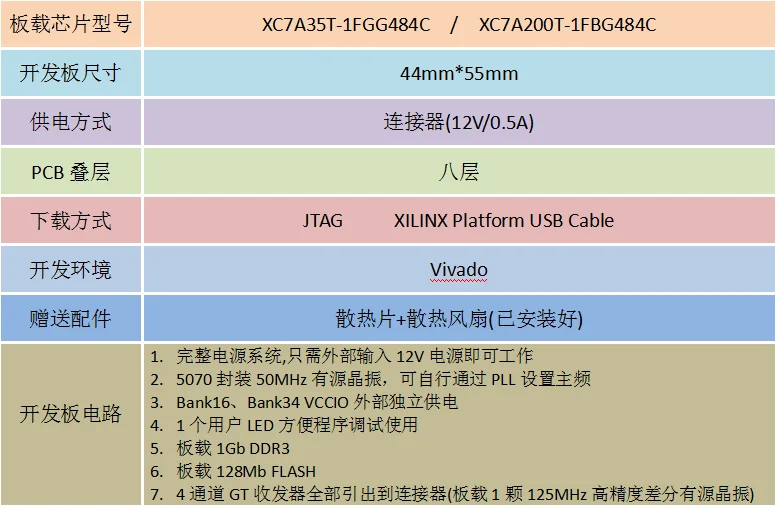
On-board chip model: XC7A35T-1FGG484C/XC7A200T-1FBG484C
Development board size: 44mm*55mm
Power supply mode: Connector (12V/0.5A)
PCB lamination: Eight layers
Download method: JTAG XILINX Platform USB Cable
Development environment: Vivado
Complimentary accessories: Heat sink + cooling fan (installed)
Development board circuit
The complete power supply system only requires an external 12V power input to operate
2.5070 package 50MHz active crystal oscillator, the main frequency can be set by yourself through PLL
3.Bank16 and Bank34 VCClO external independent power supply
4.1 User leds are convenient for program debugging and use
5. 1Gb DDR3 on-board
6. 128Mb on-board FLASH
All 7.4-channel GT transceivers are led out to the connector (with one 125MHz high-precision differential active crystal oscillator on board).
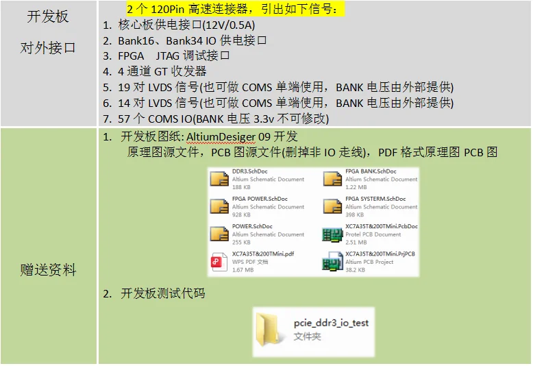
External interface of the development board
Two 120-pin high-speed connectors lead out the following signals:
Core board power supply interface (12V/0.5A)
2. Bank16, Bank34 IO power supply interfaces
3. FPGA JTAG debugging interface
4.4-channel GT transceiver
5.19 For LVDS signals (can also be used as COMS single-ended, with the BANK voltage provided externally)
6.14 For LVDS signals (can also be used as COMS single-ended, with the BANK voltage provided externally)
7.57 COMSIO(BANK voltage 3.3v, unmodifiable)
Complimentary materials
1. Development board drawings :AltiumDesiger 09 development schematic source file, PCB schematic source file (with non-IO traces removed), PDF format schematic PCB diagram
2. Test the code on the development board
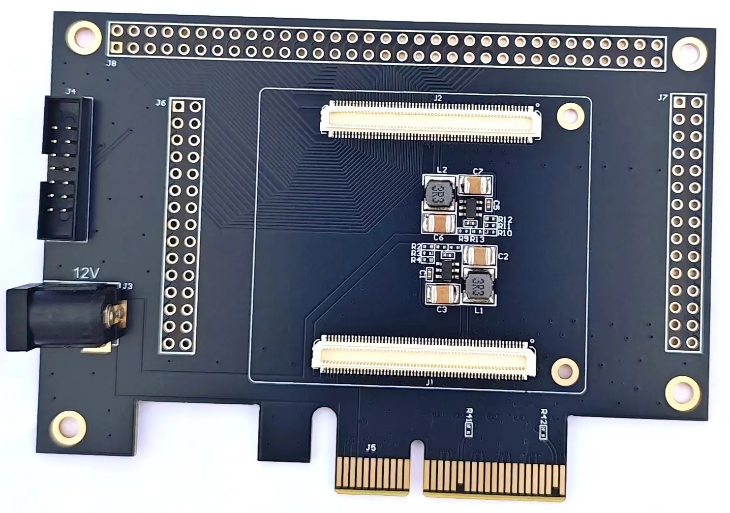
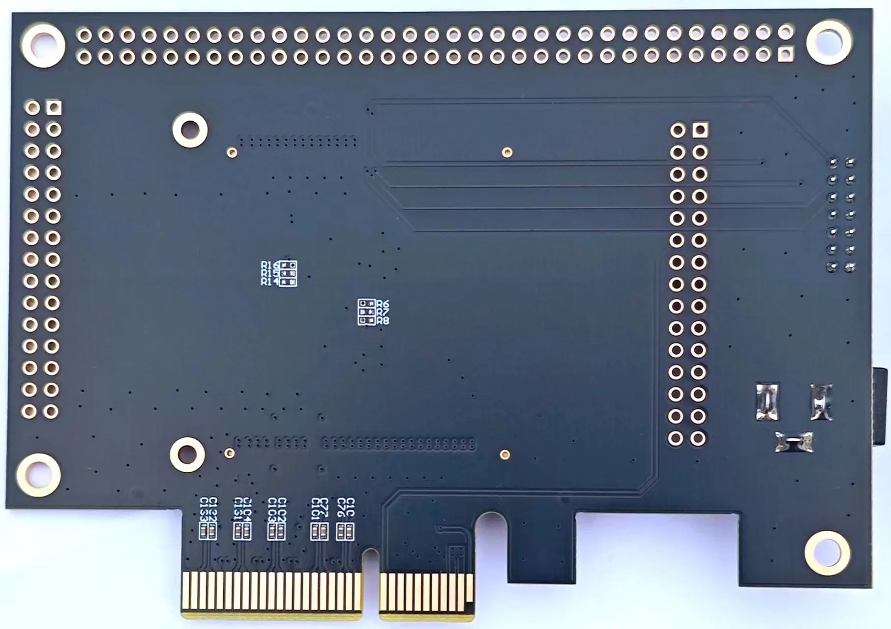
功能底板
Free Shipping Over $199
- Standard Shipping: Standard Shipping (12–18 Business Days)
- Express Shipping: Expedited Shipping (5–9 Business Days)
- Free Shipping: Orders over $199 qualify automatically
- Tracking: Full tracking number provided for all orders
30-Day Return Policy
- Returns: 30-day hassle-free return window
- Condition: Items must be unused and in original packaging
- Refund: Full refund processed within 3-5 business days
Why Choose Us?
- Factory Direct: ISO/TS 16949 certified manufacturer
- Quality: 100% electrical continuity tested before shipment
- Experience: 15+ years in automotive connector industry
- Support: Professional technical support available

You may also like
Blog posts
Title
An excerpt of your blog post's content
Title
Date|Author
Subscribe to our emails
Be the first to know about new collections and special offers.