

Compatible For J-Link OB ARM Simulation Debugger SWD Programmer STM32 Download JLink Generation V8
China Mainland
$10.72
Sale price
$10.72
Regular price
$0.00
Skip to product information


Compatible For J-Link OB ARM Simulation Debugger SWD Programmer STM32 Download JLink Generation V8
$10.72
Sale price
$10.72
Regular price
$0.00
Description
SPECIFICATIONS
Application: Computer
Brand Name: NONE
Choice: yes
Condition: New
Dissipation Power: W
High-concerned chemical: none
Operating Temperature: -40-+85
Origin: Mainland China
Supply Voltage: V
Type: Voltage Regulator
is_customized: Yes
semi_Choice: yes
Mainly Push The Most Popular Products
|
|
|
|
|
|
|
|
|
|
|
|
|
|
|
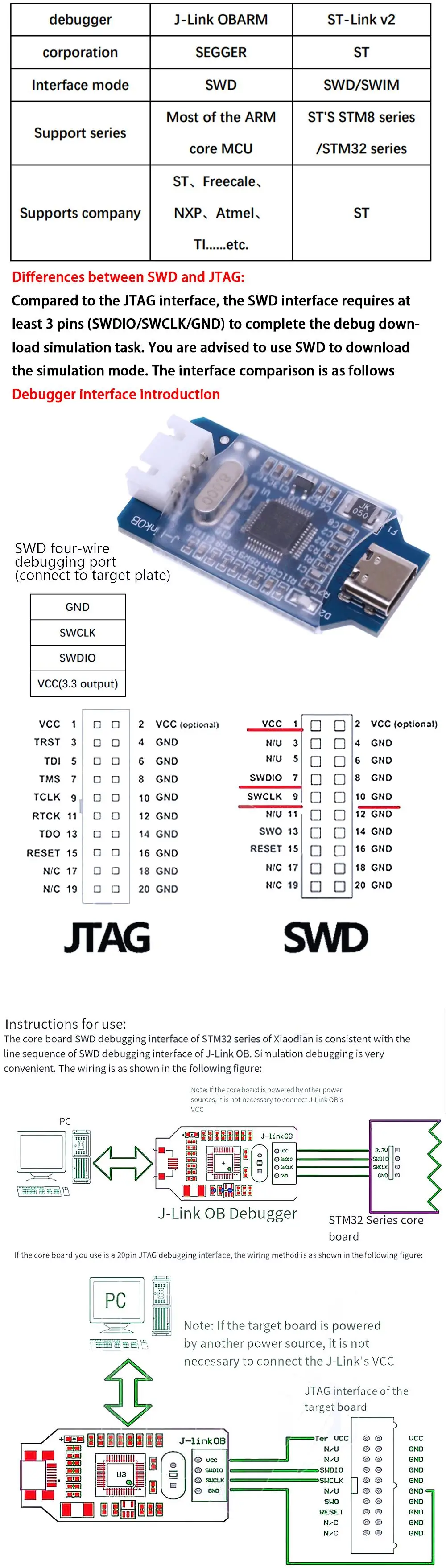
Interface description:
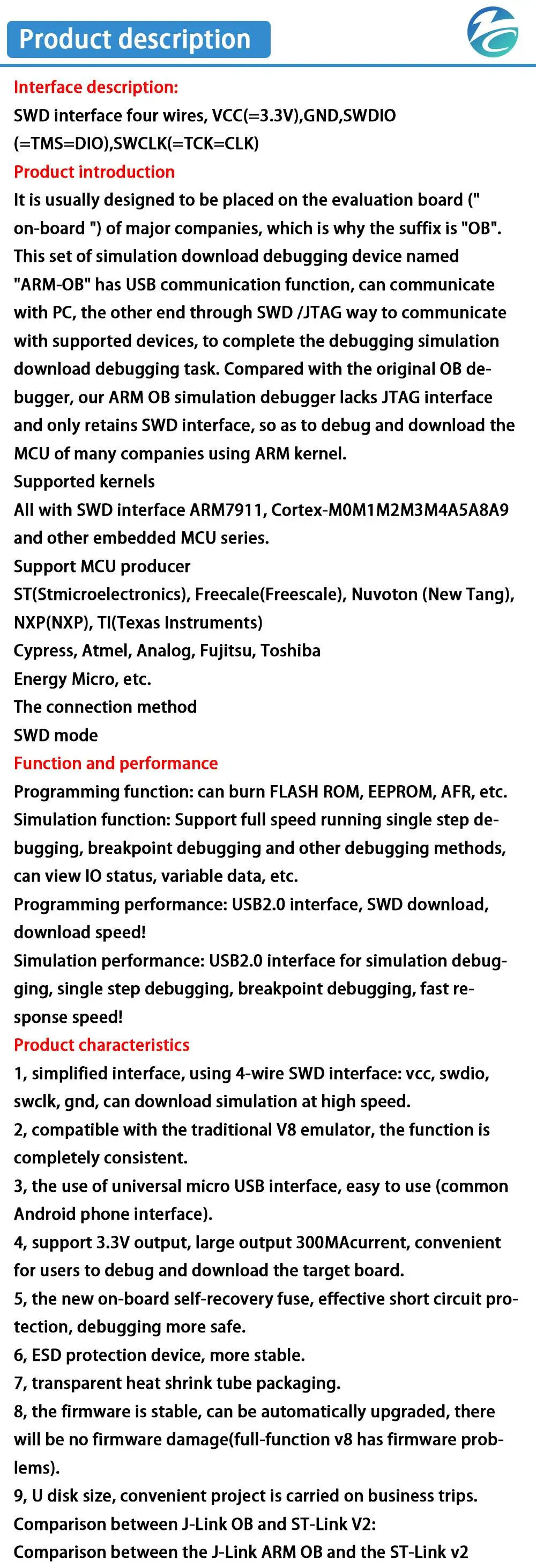
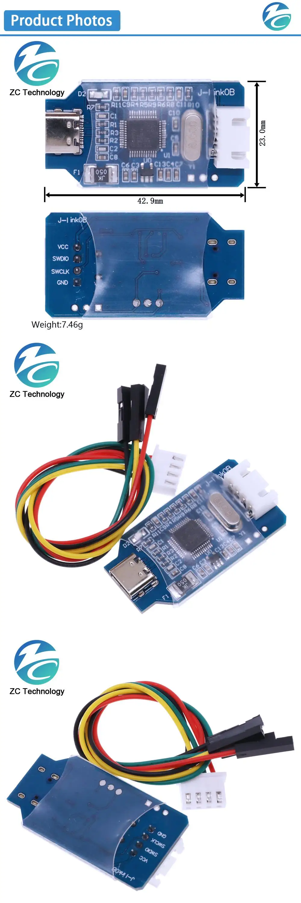
SWD interface four wires, VCC(=3.3V),GND,SWDIO(=TMS=DIO),SWCLK(=TCK=CLK)
Product introduction
It is usually designed to be placed on the evaluation board (" on-board ") of major companies, which is why the suffix is "OB". This set of simulation download debugging device named "ARM-OB" has USB communication function, can communicate with PC, the other end through SWD /JTAG way to communicate with supported devices, to complete the debugging simulation download debugging task. Compared with the original OB debugger, our ARM OB simulation debugger lacks JTAG interface and only retains SWD interface, so as to debug and download the MCU of many companies using ARM kernel.
Supported kernels
All with SWD interface ARM7911, Cortex-M0M1M2M3M4A5A8A9 and other embedded MCU series.
Support MCU producer
ST(Stmicroelectronics), Freecale(Freescale), Nuvoton (New Tang), NXP(NXP), TI(Texas Instruments)
Cypress, Atmel, Analog, Fujitsu, Toshiba
Energy Micro, etc.
The connection method
SWD mode
Function and performance
Programming function: can burn FLASH ROM, EEPROM, AFR, etc.
Simulation function: Support full speed running single step debugging, breakpoint debugging and other debugging methods, can view IO status, variable data, etc.
Programming performance: USB2.0 interface, SWD download, download speed!
Simulation performance: USB2.0 interface for simulation debugging, single step debugging, breakpoint debugging, fast response speed!
Product characteristics
1, simplified interface, using 4-wire SWD interface: vcc, swdio, swclk, gnd, can download simulation at high speed.
2, compatible with the traditional V8 emulator, the function is completely consistent.
3, the use of universal micro USB interface, easy to use (common Android phone interface).
4, support 3.3V output, large output 300MAcurrent, convenient for users to debug and download the target board.
5, the new on-board self-recovery fuse, effective short circuit protection, debugging more safe.
6, ESD protection device, more stable.
7, transparent heat shrink tube packaging.
8, the firmware is stable, can be automatically upgraded, there will be no firmware damage(full-function v8 has firmware problems).
9, U disk size, convenient project is carried on business trips.
Comparison between J-Link OB and ST-Link V2:
Comparison between the J-Link ARM OB and the ST-Link v2
Free Shipping Over $199
- Standard Shipping: Standard Shipping (12–18 Business Days)
- Express Shipping: Expedited Shipping (5–9 Business Days)
- Free Shipping: Orders over $199 qualify automatically
- Tracking: Full tracking number provided for all orders
30-Day Return Policy
- Returns: 30-day hassle-free return window
- Condition: Items must be unused and in original packaging
- Refund: Full refund processed within 3-5 business days
Why Choose Us?
- Factory Direct: ISO/TS 16949 certified manufacturer
- Quality: 100% electrical continuity tested before shipment
- Experience: 15+ years in automotive connector industry
- Support: Professional technical support available

You may also like
Blog posts
Title
An excerpt of your blog post's content
Title
Date|Author
Subscribe to our emails
Be the first to know about new collections and special offers.