

Winstar WEO012864K 31P COG Graphic SPI/I2C/6800/8080 SSD1309 3V 2.7" 27 2.7 inch 128x64 OLED Display
Yellow with Frame / China Mainland
$109.13
Sale price
$109.13
Regular price
$0.00
Skip to product information


Q: How do you manage product quality?
A: The products are baked, aging, electrical measurement and other procedures for testing.


Winstar WEO012864K 31P COG Graphic SPI/I2C/6800/8080 SSD1309 3V 2.7" 27 2.7 inch 128x64 OLED Display

Winstar WEO012864K 31P COG Graphic SPI/I2C/6800/8080 SSD1309 3V 2.7" 27 2.7 inch 128x64 OLED Display
$109.13
Sale price
$109.13
Regular price
$0.00
Description
SPECIFICATIONS
Active Area: 61.41x30.69mm
Application: High-end smart home
Brand Name: NONE
Controller: SSD1309
Display Color: Blue/White/Yellow/Green
Display Mode: 10000:1
Dot Pitch: 0.48x0.48mm
Dot Size: 0.45x0.45mm
Drive method: 1/64
High-concerned chemical: none
Interface: I2C, 4-Wire SPI ,6800, 8080
Model Number: WEO012864K
Origin: Mainland China
Panel Size: 73.0x41.86x2.11mm
Pins: 31PIN (0.5mm ZIF)
Power Supply: 3V
Resolution: 128*64,128x64 Dot Matrix
Size: 2.7 Inch
Structure: COG
Type: Graphic,PMOLED
View Angel: Full View
is_customized: Yes

1.Specification parameters
Model No. WEO012864K
►Type: Graphic
►Structure: COG; Frame Option
►Size: 2.7 inch
►128 x 64 Dot Matrix
►IC:SSD1309
►3V Power supply
►1/64 duty
►Interface: 6800, 8080, SPI, I2C
►Display Color: White / Yellow / Sky Blue / Green
►Other FPC options available in below table
Description
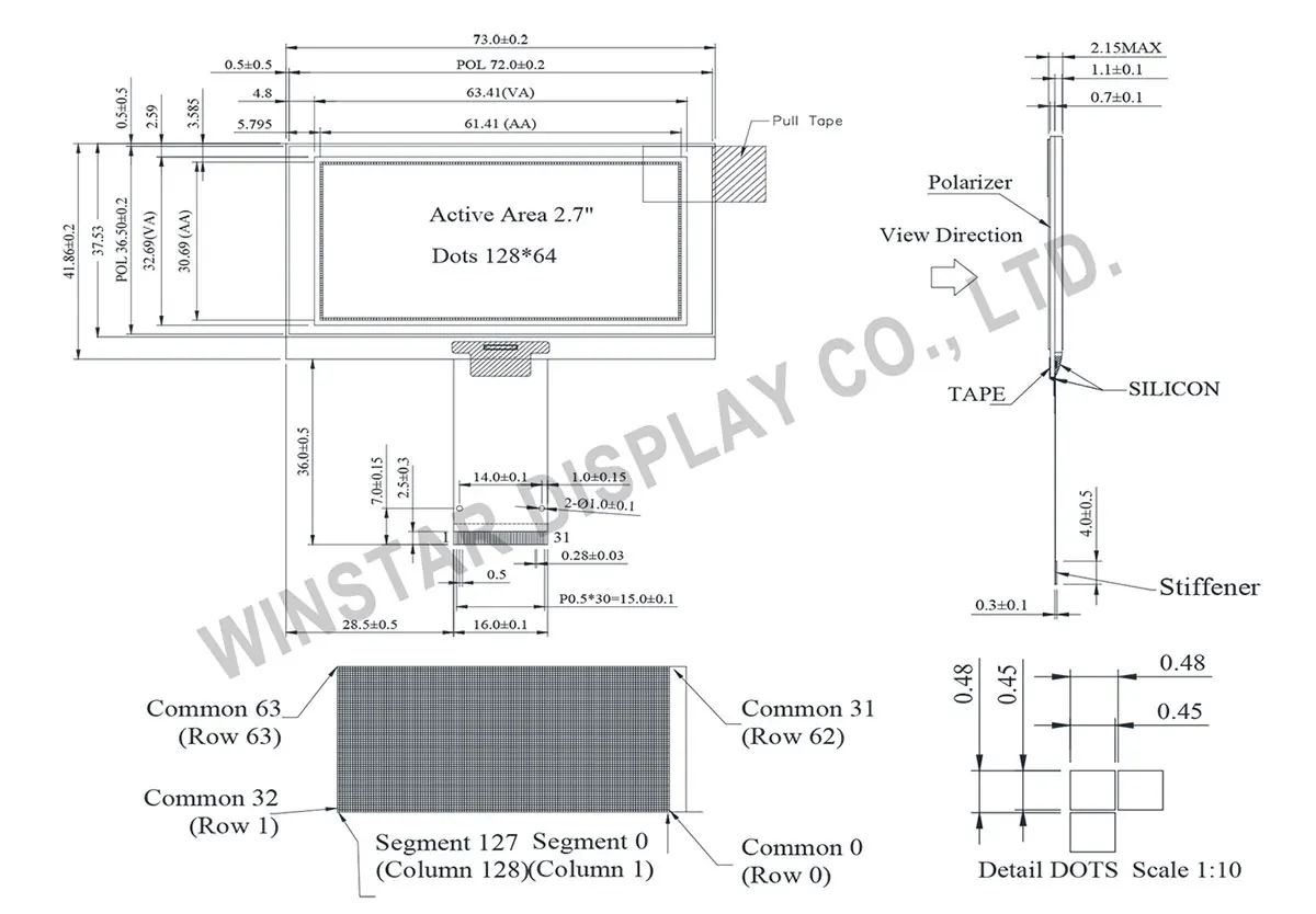
Winstar OLED Monochrome Display WEO012864K is made of 128x64 pixels, diagonal size is 2.7 inch. This graphic display is built-in SSD1309 IC which with the module dimension of 73.0 x 41.86 mm and AA size of 61.41 x 30.69 mm. The display is based on a chip-on-glass technology and therefore reaches a very low installation depth of only 2.15 mm.
2.Extenal Dimensions
3.Pin Descriptions
Interface Pin Function
No. |
Symbol |
Function |
|||||||||||||||
1 |
NC(GND) |
No connection |
|||||||||||||||
2 |
VSS |
Ground. |
|||||||||||||||
3-10 |
NC |
No connection |
|||||||||||||||
11 |
VDD |
Power supply pin for core logic operation |
|||||||||||||||
12 |
BS1 |
MCU bus interface selection pins. Select appropriate logic setting as described in the following table. BS2, BS1 and BS0 are pin select
Note
(1) 0 is connected to VSS (2) 1 is connected to VDD |
|||||||||||||||
13 |
BS2 |
||||||||||||||||
14 |
NC |
No connection |
|||||||||||||||
15 |
CS# |
This pin is the chip select input connecting to the MCU. |
|||||||||||||||
16 |
RES# |
This pin is reset signal input. |
|||||||||||||||
17 |
D/C# |
This pin is Data/Command control pin connecting to the MCU. |
|||||||||||||||
18 |
R/W# |
This pin is read / write control input pin connecting to the MCU interface. |
|||||||||||||||
19 |
E/RD# |
This pin is MCU interface input. |
|||||||||||||||
20~27 |
D0~D7 |
These pins are bi-directional data bus connecting to the MCU data bus. |
|||||||||||||||
28 |
IREF |
This pin is the segment output current reference pin. |
|||||||||||||||
29 |
VCOMH |
COM signal deselected voltage level. |
|||||||||||||||
30 |
VCC |
Power supply for panel driving voltage. This is also the most positive power voltage supply pin. |
|||||||||||||||
31 |
NC(GND) |
No connection |
Electronical Characteristics
Drawing |
Reference Part Number |
Material |
Detailed Drawing |
|
WEF012864K* |
SUS-304 |
spec drawing |
Frame Option:
Item |
Symbol |
Condition |
Min |
Typ |
Max |
Unit |
Supply Voltage for Logic |
VDD |
- |
2.8 |
3.0 |
3.3 |
V |
Supply Voltage for Display |
VCC |
- |
12 |
13 |
14 |
V |
High Level Input |
VIH |
- |
0.8×VDD |
- |
- |
V |
Low Level Input |
VIL |
- |
- |
- |
0.2×VDD |
V |
High Level Output |
VOH |
- |
0.9×VDD |
- |
- |
V |
Low Level Output |
VOL |
- |
- |
- |
0.1×VDD |
V |
50% Check Board operating Current |
VCC =13.0V |
- |
22 |
33 |
mA |
|
Absolute Maximum Ratings
Parameter |
Symbol |
Min |
Max |
Unit |
Supply Voltage for Logic |
VDD |
-0.3 |
4 |
V |
Supply Voltage for Display |
VCC |
0 |
15 |
V |
Operating Temperature |
TOP |
-40 |
+80 |
°C |
Storage Temperature |
TSTG |
-40 |
+85 |
°C |
General Specification
Item |
Dimension |
Unit |
Dot Matrix |
128 x 64 |
- |
Module dimension |
73.0 × 41.86 × 2.11 |
mm |
Active Area |
61.41 × 30.69 |
mm |
Pixel Size |
0.45 × 0.45 |
mm |
Pixel Pitch |
0.48 × 0.48 |
mm |
Display Mode |
Passive Matrix |
|
Display Color |
Monochrome |
|
Drive Duty |
1/64 Duty |
|
Interface Pin Function
No. |
Symbol |
Function |
|||||||||||||||
1 |
NC(GND) |
No connection |
|||||||||||||||
2 |
VSS |
Ground. |
|||||||||||||||
3-10 |
NC |
No connection |
|||||||||||||||
11 |
VDD |
Power supply pin for core logic operation |
|||||||||||||||
12 |
BS1 |
MCU bus interface selection pins. Select appropriate logic setting as described in the following table. BS2, BS1 and BS0 are pin select
Note
(1) 0 is connected to VSS (2) 1 is connected to VDD |
|||||||||||||||
13 |
BS2 |
||||||||||||||||
14 |
NC |
No connection |
|||||||||||||||
15 |
CS# |
This pin is the chip select input connecting to the MCU. |
|||||||||||||||
16 |
RES# |
This pin is reset signal input. |
|||||||||||||||
17 |
D/C# |
This pin is Data/Command control pin connecting to the MCU. |
|||||||||||||||
18 |
R/W# |
This pin is read / write control input pin connecting to the MCU interface. |
|||||||||||||||
19 |
E/RD# |
This pin is MCU interface input. |
|||||||||||||||
20~27 |
D0~D7 |
These pins are bi-directional data bus connecting to the MCU data bus. |
|||||||||||||||
28 |
IREF |
This pin is the segment output current reference pin. |
|||||||||||||||
29 |
VCOMH |
COM signal deselected voltage level. |
|||||||||||||||
30 |
VCC |
Power supply for panel driving voltage. This is also the most positive power voltage supply pin. |
|||||||||||||||
31 |
NC(GND) |
No connection |
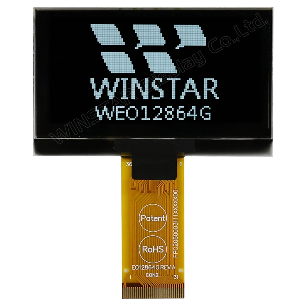
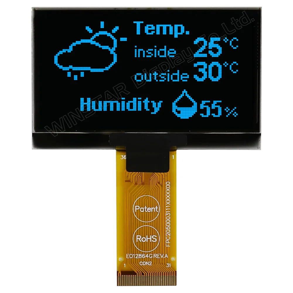
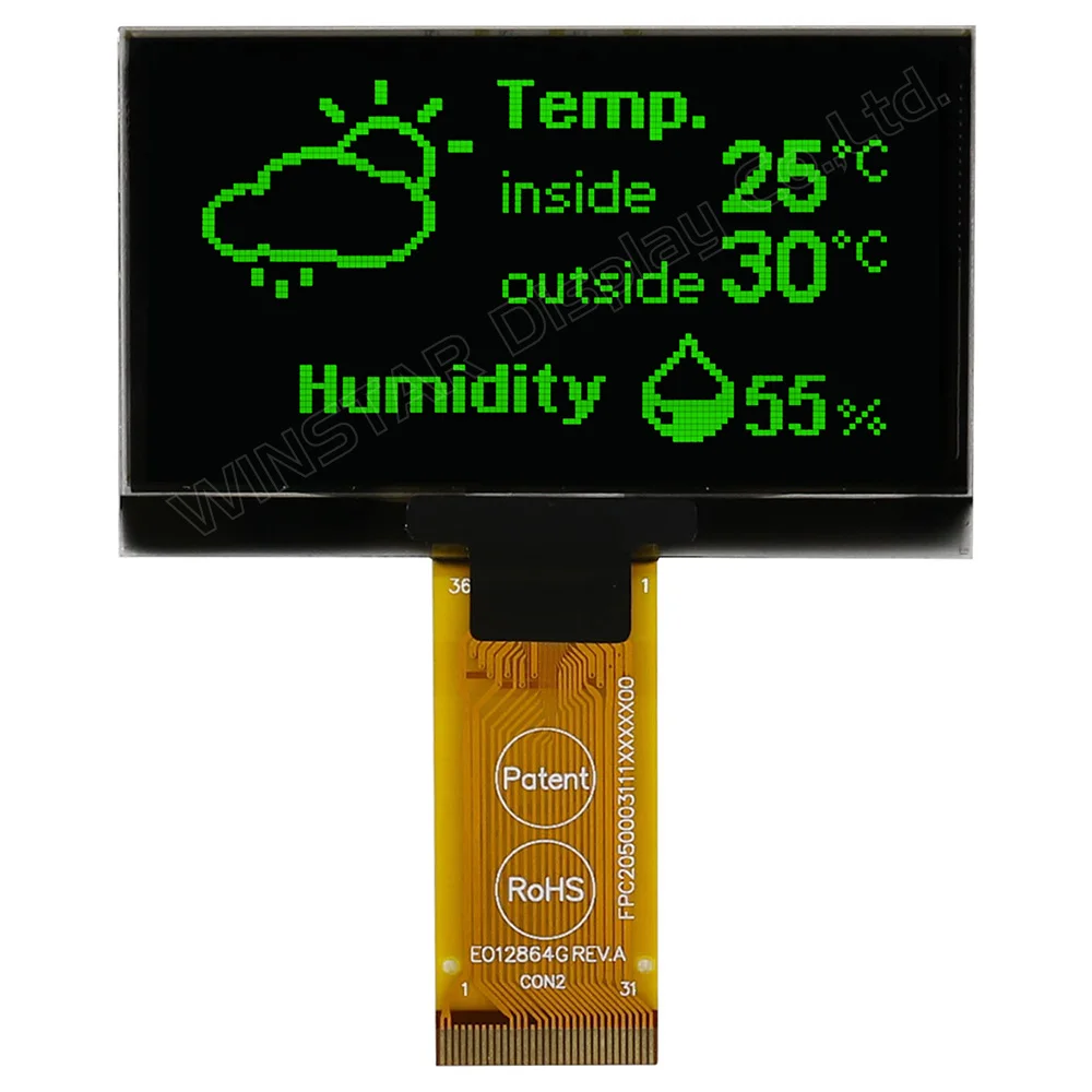
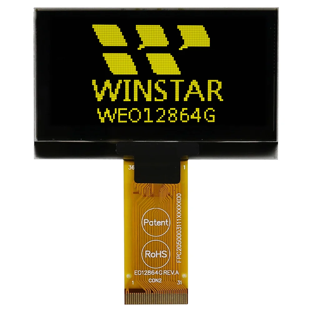
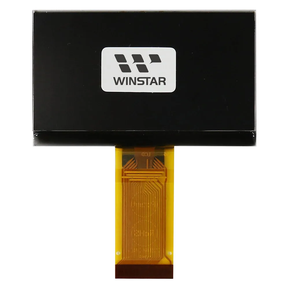
4.Photo Display


Q: Is the product in stock? How long production cycle?
A: Some products are in stock, Small batch production for 1-2 weeks,Mass production for 3-4 weeks.
Q: How long is the product warranty and service?
A: The product is valid for 1 year and is a lifetime technical support service.
Q: Can you customize the product? How can I get the samples?
A: We can customize as needed, and the quantity has a minimum order quantity requirement.
A: Some products are in stock, Small batch production for 1-2 weeks,Mass production for 3-4 weeks.
Q: How long is the product warranty and service?
A: The product is valid for 1 year and is a lifetime technical support service.
Q: Can you customize the product? How can I get the samples?
A: We can customize as needed, and the quantity has a minimum order quantity requirement.
Send inquiry → Offer quotation →Confirm quotation & pay tooling charge → Provide drawing → confirm drawing → make tooling &samples → Samples finished → Delivery via freight or sea collect.
Q: Can you provide drawings and related procedures?
A: We can provide drawings and procedures for customers to confirm.
Q: Can the LCD module be Export directly?
A: The products are through the relevant certification, it can be exported.
Q: Are you manufactory or trade company?
A:We are professional manufactory, which specializes in TN, HTN, FSTN, STN monochrome LCD, LED backlights, LCD modules more than 10 years.
A: We can provide drawings and procedures for customers to confirm.
Q: Can the LCD module be Export directly?
A: The products are through the relevant certification, it can be exported.
Q: Are you manufactory or trade company?
A:We are professional manufactory, which specializes in TN, HTN, FSTN, STN monochrome LCD, LED backlights, LCD modules more than 10 years.
Q: How do you manage product quality?
A: The products are baked, aging, electrical measurement and other procedures for testing.
Free Shipping Over $199
- Standard Shipping: Standard Shipping (12–18 Business Days)
- Express Shipping: Expedited Shipping (5–9 Business Days)
- Free Shipping: Orders over $199 qualify automatically
- Tracking: Full tracking number provided for all orders
30-Day Return Policy
- Returns: 30-day hassle-free return window
- Condition: Items must be unused and in original packaging
- Refund: Full refund processed within 3-5 business days
Why Choose Us?
- Factory Direct: ISO/TS 16949 certified manufacturer
- Quality: 100% electrical continuity tested before shipment
- Experience: 15+ years in automotive connector industry
- Support: Professional technical support available

You may also like
Blog posts
Title
An excerpt of your blog post's content
Title
Date|Author
Subscribe to our emails
Be the first to know about new collections and special offers.